
NanoChemLab group is affiliated to CNRS and UM and is located at the Electronic Institute of Montpellier (IES) within the Saint Priest campus, which includes renowned centers in sensors devices, materials science, microelectronics and robotics, among others.
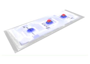
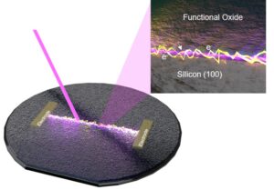
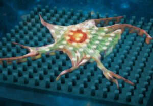
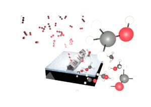
The NanoChemLab group is developing a wide range of sensors and actuators based on our materials development, such as biological sensors, radioactivity sensors, optical position sensors covering the visible to near infrared range, energy harvesters and catalytic devices for CO2 reduction. The team also specialises in bottom-up and top-down micro- and nanostructuring of devices for biological or energy applications. Overall, the research activity of the team goes from material synthesis to prototyping, thanks to our expertise in electronic instrumentation systems. This feature, allowed the NanoChemLab to expand its activity through the creation of a start-up and technology transfer.
This activity is divided into 5 research themes to investigate the physical phenomena such as piezoelectricity, ferroelectricity, photovoltaics and the catalytic effect of our oxides:

Research Methodology
The research methodology of the NanoChemLab team, is focused on developing and manufacturing processes for novel functional oxide nanomaterials integrated into silicon and devices. To develop these activities, the team counts on different specialized laboratory spaces to achieve the integration of epitaxial oxide thin films and nanostructures on silicon up to 6-inch and device prototyping.
These laboratory spaces comprise a molecular chemical synthesis laboratory, where the chemical precursors of the nanomaterials to be synthesized are prepared. Then, the team has established a laboratory for the deposition of chemical solutions and nanostructures where thin films and nanomaterials on silicon are fabricated from the chemical precursor solutions. Importantly, NanoChemLab has developed a know-how in alternative lithography techniques (soft nanoimprint lithography and silicon-chemical etching systems), which allows us to produce submicron structures collectively and at a lower cost out of the clean room. We also developed instrumentation and chemical solution deposition systems such as a dip-coater and spin-coater equipped with a glovebox to manipulate objects and coating solutions in a separate and controlled atmosphere. After deposition, the materials are crystallized in a crystal growth laboratory, equipped with advanced tubular furnaces with atmosphere control and diameter up to 6-inches.

The synthesized materials are then characterized in our structural characterization laboratory equipped with state-of-the-art equipment such as 2D X-ray diffractometer (model Bruker D8 Advance A25) with a 2D detector to control de crystal oxide quality and homogeneity up to 4-inch silicon wafer. Once characterized, our material is micro- or nano-processed in the clean room of the University of Montpellier, located in the same building as the IES. Notably, the team is an advanced user and has participated in setting up MEMS microfabrication devices at the CTM, a microfabrication platform on-site. The CTM has a clean room of 400 m2 and a set of recent machines (machines of deposit, engraving, lithography, and lithography and metrology) acquired thanks to a grant from Europe (ERDF). The clean room allowed us to develop advanced MEMS and prototypes. Finally, the team counts, thanks to its funding, with a laboratory to carry out advanced physical and electrical characterization such as vibrational characterization thanks to a novel measuring system for MEMS structures capable of high-frequency non-contact vibration analysis with high precision from Doppler-type interference phenomenon (SLDV) up to 2.5GHz (polytec MSA600 microsystem analyser).